Semiconductor Device & Failure Analysis - Using Photon Emmission Microscopy, 1st Edition
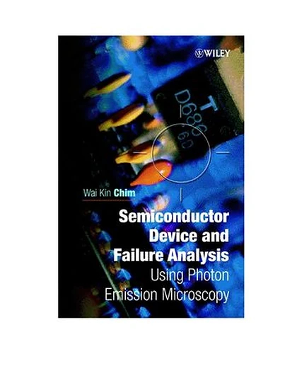
Semiconductor Device & Failure Analysis - Using Photon Emmission Microscopy, 1st Edition
Summary
The diminishing size and greater complexity of modern semiconductor integrated circuits poses new challenges in fault detection. Photon Emission Microscopy (PEM) is a physical fault localisation technique used for analysing IC failures. Detailing the PEM technique and its application to semiconductor device analysis, this unique reference: * Illustrates the application of the PEM technique in various areas of device reliability, in particular hot-carrier, oxide and ESD reliability. * Presents the principles of design and calibration for a spectroscopic emission microscope system along with coverage of the three main operation modes: frontside, backside and spectroscopic PEM * Provides an analysis of light emission in semiconductors under hot-carrier and high-field impulse stressing in MOS transistors and photon emission from biased MOS capacitors. Not only an essential refere